· via Hacker News – Front Page (native)
Samsung and XCENA's MX1 pairs 2 TB CXL memory expansion with 3072 RISC-V cores
At Hot Chips 2026, XCENA and Samsung detailed MX1, a CXL 3.2 memory expansion card with up to 2 TB of DDR5, SSD-backed "Infinite Memory" and 3072 RISC-V cores for near-memory compute.
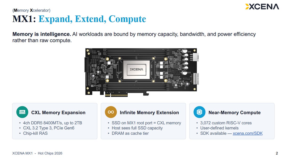
A CXL card that expands, stores and computes
At Hot Chips 2026, XCENA and Samsung presented the MX1, a PCIe add-in card whose name stands for "Memory Xcelerator". According to Chips and Cheese, the device plays three roles at once: it expands host memory over CXL, it can attach SSDs and expose them as memory, and it carries a large compute engine of its own.
On the expansion side, the card accepts up to 2 TB of DDR5 and connects to the host over a PCIe 6 / CXL 3.2 x8 link, providing 128 GB/s of aggregate bandwidth, or 64 GB/s in each direction. Eight downstream PCIe 6 lanes are available for SSDs, and attached storage can be presented to the host as CXL memory with the card's DRAM acting as a cache, a capability XCENA brands as "Infinite Memory".
3072 RISC-V cores for data-parallel work
The onboard compute is the design's most distinctive feature. Chips and Cheese reports that the chip integrates 3072 RISC-V cores organised in clusters of 32 that share L2 caches and a data TLB. Four clusters form a subsystem, the smallest unit of job allocation, and with 24 subsystems the card can run 24 independent jobs concurrently. An in-house network-on-chip ties the subsystems to L3 cache and memory, while two Arm Cortex A53 cores handle control functions.
The RISC-V cores are in-order and clocked at 1.1 GHz, a throughput-first strategy the article compares to Intel's Xeon Phi: many modest cores attacking highly parallel tasks where exploiting memory bandwidth and power efficiency matters more than single-threaded speed. The power figures underline that focus. Fabricated on Samsung's 4nm process, the chip draws 40 W, which works out to a bit under 13 mW per RISC-V core, and the board consumes 90 W with four DIMMs fitted.
A GPU-like memory hierarchy
The cache hierarchy is unusual. Each core has a 4 KB virtually addressed L1 data cache, so data accesses skip address translation on a hit. Clusters share a 128 KB L2 data cache that is virtually indexed and physically tagged, along with a shared TLB holding 1024 entries for 64 KB pages and 8 entries for 1 GB pages. On the instruction side, groups of four cores share an 8 KB instruction cache, backed by a 128 KB cluster-level L2 instruction cache, and instruction fetches run directly on physical addresses with no virtual memory at all. The program counter is restricted to predefined device physical code regions, which keeps cores from accidentally executing data, and jobs are isolated from each other at subsystem boundaries.
The programming model resembles OpenCL or CUDA: a kernel is invoked many times, with each instance using an index, mu::getTaskIdx(), analogous to OpenCL's get_global_id(), to decide what data to process. The device also shares virtual addresses with the host, so host and MX1 code can pass pointers back and forth much like OpenCL's shared virtual memory, with XCENA's software maintaining matching page tables.
XCENA also exploits RISC-V's extensibility with a custom Vector Processing Engine at the subsystem level. Each core gets a VPE command queue and can offload vector operations, with the VPEs supporting FP32 and FP16 and delivering roughly 3 TFLOPS of dot-product throughput across the chip. Notably, integer operations are not accelerated, and the API exposes the vector unit through built-in functions that return error codes rather than raising exceptions, so code must check for overflow and invalid accesses explicitly.
SSD-backed memory with DRAM caching
The "Infinite Memory" tier works by exposing attached SSDs as CXL memory. SSDs can be run in RAID, and because downstream and upstream bandwidth are matched, the card can in principle saturate its host link using SSDs alone. To blunt SSD latency, the onboard DDR5 caches SSD contents in 64 KB pages, tracked by a 1024-entry on-chip map cache; a miss triggers a page fault handled by firmware running on the MX1's own cores, which fetches data from the SSD and updates the mapping. Chips and Cheese flags an inconsistency it cannot resolve here: 1024 entries at 64 KB pages covers only 64 MB, yet XCENA's documentation says the cache defaults to 16 GB with capacity adjustable in 16 MB steps.
A complementary "pinned prefix" mechanism lets users pin a contiguous region of SSD-backed addresses into DRAM, sized in 16 MB steps. Because it is a prefix rather than arbitrary pages, it suits keeping a hot buffer resident; XCENA's own example pins 115.5 GB out of 231 GB of attached DRAM.
Why it matters
Machine learning workloads keep outgrowing conventional memory capacity, and MX1 is an attempt to answer that from a standard PCIe slot: pooled DRAM, an SSD tier that behaves like memory, and thousands of small cores placed next to the data so that work moves to memory instead of memory contents streaming across the host link. The architecture also signals where CXL is heading, from passive capacity toward memory with compute attached. Questions remain, including SSD-tier latency, the map-cache discrepancy, and the maturity of the software stack, and the Hot Chips disclosure covered by Chips and Cheese says nothing about availability or pricing. As a design point, though, it shows how far memory expansion devices are evolving beyond simple capacity add-ons.
- #cxl
- #risc-v
- #samsung
- #memory-expansion
- #datacenter