· via Hacker News – Front Page (native)
Samsung's LPDDR5X-PIM embeds AI compute in DRAM banks at Hot Chips 2026
At Hot Chips 2026, Samsung presented LPDDR5X-PIM, DRAM with MAC units in every bank that reaches 614 GB/s of internal bandwidth while staying compatible with standard memory controllers — if software can handle it.
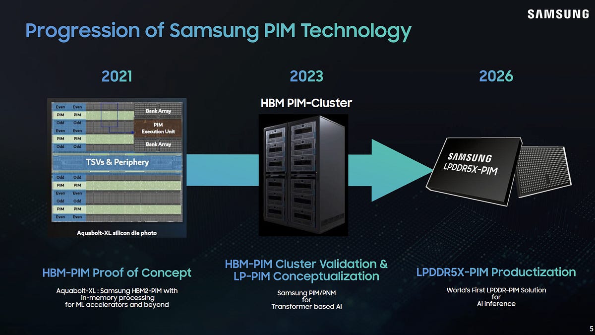
What Samsung presented
At Hot Chips 2026, Samsung presented its continued push into processing-in-memory (PIM), a design that embeds multiply-accumulate (MAC) units directly inside LPDDR5X DRAM chips. As Chips and Cheese reports, the approach attacks two long-standing bottlenecks at once: compute placed inside a memory chip can exploit far higher internal bandwidth, and it sidesteps the slow round trip between memory and conventional cores.
The bandwidth argument
A normal DRAM access is limited by the chip's external interface. Even if a memory controller activated every bank simultaneously, it could not drain the bandwidth available across all of them. Samsung's LPDDR5X-PIM is essentially a standard LPDDR5X-9600 part with 16 banks, but each bank gets its own PIM block that reads data without going through the external bus. According to figures cited by Chips and Cheese, the blocks together can use 614 GB/s of internal bandwidth, while regular DRAM accesses — which touch at most two banks in parallel — top out at 76.8 GB/s.
Inside a PIM block
Each PIM block is a MAC tree surrounded by register files and control logic. A 1024-bit instruction register file holds up to 64 16-bit instructions, and a 4 kbit source register file stores activation vectors, supplying one operand to the MAC array. The second operand comes from the attached DRAM bank, reflecting Samsung's assumption that software loads model weights into DRAM. A 2 kbit scale register provides factors for scaling weights before computation.
The MAC array targets low-precision AI formats. Numbers from Samsung's presentation indicate four INT8 or FP8 MACs per data clock for each block, with throughput doubling for 4-bit input weights, for a package-wide total of 2.4 TOPS. That is modest on its own, but Chips and Cheese points out that eight chips would reach 9.6 INT8 TOPS — roughly on par with the NPU in Intel's Meteor Lake — at the cost of 128 GB of memory.
Compatibility through reserved rows
The design's most interesting property is that it keeps the chip inside the standard LPDDR5X protocol while adding behaviour the memory standard never defined. Samsung reserves special row addresses that work something like MMIO addresses. A pair of predefined rows per channel switches the chip between single-bank mode, which is normal operation, and multi-bank mode, which broadcasts commands across all 16 banks. Additional per-bank rows flip read and write commands to target PIM registers instead of DRAM contents.
The intended workflow: load weights into DRAM in single-bank mode, switch to multi-bank mode with PIM registers activated, then write activation values, scale factors and instructions — each write broadcast to all 16 banks at once. That broadcast matters because a DRAM packet is only 256 bits, so filling a source register takes 16 write commands, and doing that bank by bank across 16 banks would make host-side register writes the bottleneck. Subsequent read commands trigger computation and accumulate results into PIM vector register files, and write commands push results back into DRAM. An Address Align Mode lets each instruction infer its source register index from the column address, so computation still works when the memory controller reorders accesses. Results are retrieved by switching back to single-bank mode. Samsung reported substantial internal performance gains over standard LPDDR5X.
The software problem
The same mechanism creates the architecture's steepest obstacle. Because PIM modes redefine what DRAM commands mean, a system cannot run PIM compute and ordinary memory traffic at the same time — not even across threads, since memory controllers and DRAM chips have no notion of which thread an access belongs to. A stray read from a non-PIM thread could trigger unintended computation and corrupt results; a stray write could send vector register data to the wrong address.
Samsung's answer is to isolate a PIM region in memory, but Chips and Cheese sees no cheap way to do it: designating whole channels as PIM-only would break address interleaving, cutting bandwidth for normal applications while PIM code loses the compute of the remaining channels. Locking and OS-level coordination problems would remain on top of that.
Why it matters
The memory wall is the defining constraint on AI inference, and Samsung is demonstrating that compute can be moved into the memory chip itself without abandoning standard interfaces — a genuine engineering achievement that could shorten the path to commercial adoption. The raw compute per package is modest and the programming model is hostile to multitasking systems, so PIM is unlikely to displace NPUs or GPUs soon. But as a way to reclaim bandwidth that conventional architectures leave stranded inside DRAM, LPDDR5X-PIM is one of the more credible attempts yet, and how Samsung resolves the software obstacles will decide whether in-memory compute ever leaves the lab.
- #samsung
- #processing-in-memory
- #dram
- #ai-chips
- #hardware